

Buy the PCB:

DOCUMENTS:
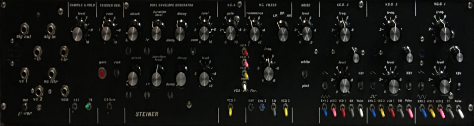
FUNCTION:
On receiving a trigger, this module samples and holds the voltage present at the input or from the internal random voltage generator until a new trigger is received. This held voltage can be used as a control voltage for any module which accepts a control voltage. EG: VCO, VCA, VCF, Sequence clock, etc.
From the Synthasystem manual:
Each S&H module, upon application of a trigger to its input jacks will step to a new and randomly chosen D.C. output voltage and hod at that level until the next trigger occurs.
Each S&H has two output jacks in parallel.
The output voltage range of each S&H can be compressed to zero or turned to maximum by adjusting the level pot ont he front panel.
The input trigger duration is irrelevant to the operation of the S&H.
Sample waveforms illustrating the operation of the S&H are shown at the top of figure #11A.

Figure #11A
USE:
This module can be used to create random or deterministic control voltages from the internal random voltage generator or a user supplied input signal. There are two modules behind the panel. The trigger and signal input are normaled such that a signal or trigger connected to the first S&H will also be sent to the second S&H. This normalization is broken if a plug is inserted into the second S&H trigger or signal input jack.
Inputs/Outputs:
This module has two inputs and one output:
- Each S&H has a signal input
- Each S&H has a trigger input
- Each S&H has a signal output
Knobs:
This module has 1 knob:
- Each S&H has an output attenuator control
Switches:
There are no switches other than the switched jacks used on the input jacks. If you want, you can use a manually activated normal switch as was done on the original module.
GENERAL CONNECTIONS:
The connections are Straight forward. The simplest is to just connect the output to the module you want to control, connect a trigger source to the trigger input, and let it run. You should get a random control voltage at the output which changes at each trigger.
You can also provide your own signal source which will be sampled and held at each trigger.
For example, you can use a low frequency saw, ramp, or triangle signal for the input and create a stair step output by sampling at a higher frequency than the input signal.
COMPONENT SELECTION:
See the Component Notes page for more information.
Resistors:
This module was originally built with carbon core, 5% resistors with one or two 1% metal film resistors. So, you have a wide range of options here. I recommend using 1% tolerance, metal film resistors everywhere, but the critical resistors are R37 and R38, input summing resistors. These should ideally be hand matched or purchased to 0.1% tolerance to insure consistent response between the inputs.
Capacitors:
There are probably a billion different ceramic capacitors at a place like Mouser. Pick a capacitor that can fit the hole easily, typically 0.1 inch on centers.
Pick good quality electrolytics where designated.
C5 and C6 need to be a thermally stable, low leakage capacitor. A good polystyrene cap will work. If you can’t find a polystyrene, a polypropylene is a good substitute. The quality of the capacitor will significantly affect how long the sample can be held effectively.
Transistors:
The original used 2N5172 NPN and 2N5138 PNP transistors. These are still available, but I could only find a “PN5138” which I think is the same transistor. In any event, you can use any standard NPN or PNP transistors and they should work.
The original used 2N5163 JFETs, but as described elsewhere, there were some quality problems with the 5163s so they went to a 2N5246. These are still in production and work splendidly.
You will note the schematic has a “guard ring” designated around the high impedance nodes to reduce leakage currents and therefore drooping in the output. I found by isolating these components from the others on the PCB and spreading out the legs of the FET there was negligible droop and it all works fine.
You need a couple of unijunction transistors. These are archaic beasts which have been mostly replaced by the 555 chip. These aren’t impossible to find, but they can be pricey. The original modules used a 2N4891 which is hard to get.
For a unijunction Transistor (UJT), I found a 2N4871 or an NTE6409 work best. I’ve tried several different ones and they don’t work with the components Nyle specified. You can get both parts at Newark/Farnell. The 2N4871 is about $1.00 US and the 6409 is about $7.00.
You can buy the 2n4891s at Nikko:
They are EXPENSIVE! But they seem to be the real deal. I bought and they seem to work fine.
Diodes
Nothing special, 1N4001 type and standard LEDs are fine.
Pots
Your choice for your panel. If you use the panel I laid out, the holes and spacing will work for the Alpha 12 and 16mm pots. You can probably use nicer BTI, Bourns, etc. 9mm pots with “pot chiclets”
Trimmers
Use good trimmers, please. A good Bourns multi-turn trimmer like Bourns 3296Y series will fit the pad layout and work well.
Jacks
For the panel I laid out, a good 3.5mm or 1/8 inch jack will work. I use the Switchcraft 42A Tini-Jax true 1/8 inch jack. These are switched jacks and they work with 1/8 inch plugs and 3.5 mm plugs.
Switches:
I’m using an Electroswitch C5P0112N-A Mouser number is: 690-C5P0112N-A for the rotary switch. It can be set to any number of throws from 1 to 12.
BUILD NOTES:
Soldering:
I assume you know the basics of soldering. I like to insert the low lying parts first, like resistors, diodes, etc. After these, I install the IC sockets. Next capacitors, transistors, connectors. Use a good solder, either an organic flux, which you should wash regularly, or a no-wash flux.
Take a break every so often, wash off the flux if you are using a flux which required cleaning. Double and triple check orientations, pins, and solder joints.
Power Supply Regulation/Filtering:
Some additional comments here. These modules are tested to run on +/-12 VDC. The original power supply in the Synthasystem was +12/-10 VDC due to how Nyle designed the -10 volt section of the power supply, not for any magical requirement to have -10 volts.
The power/regulation section has 2 voltage regulators on it which can be set to +12/-10 (or +/-12 volts) depending on your needs. If you are coming from +/-15 volts, you need both regulators and you may as well set one to -10 volts.
If you are coming from +/-12 volts, technically you don’t need the regulators, but if you want, install the negative one and set it to -10 volts. The LEDs are not strictly needed. They are there to establish a base current draw so the regulators will work.
Important… if you don’t install the regulators, you have to install a jumper between pins 2 and 3 as shown on the Power/Regulation PCB or you won’t get power.
COMPONENT PLACEMENT:
I’ve learned a lot while designing this PCB, and while you are locked into the PCB mounting configuration, I’d like to add some explaination as to why some parts are where they are.
First, you’ll note there are three holes for the Polystyrene capacitor, C5 and C6. I did this to hopefully help accomadate different sizes of capacitors, so please note two of the holes, the two closest together, are connected, so pick the one which best fits your capacitor.
Next, you’ll see I’ve spread out the legs of the FETs. and clustered the gate of Q7, Q8 source of Q11,Q12, R13, R14, and one side of C5,6 close together. The schematic shows these pads surrounded by a guard ring which is connected to to the emitter of Q9 or Q10. These nodes are at called “high impeadence” nodes and as such, if there is any lower impeadence path to a lower voltage potential, these nodes will leak to that potential. A guard ring which has the same potential and is at a low impeadence node will help the voltage at the high impeadence nodes “hold”. Q9, Q10 act as a voltage follower and so the emitter will be a low impeadence at a voltage basically a diode drop from the voltage at the high impeadence nodes.
The prototype PCB does not have a guard ring on the suggestion of Nyle, so I just tried to put the high impeadence nods as close to each other as physically reasonable (I could have put R13, R14 on end, but chose not to) and then put the other tracks and nodes far away. I haven’t built the prototype yet, but if it works this way, I’ll leave it. If the voltage bleeds off, I’ll try the guard ring.
MOUNTING:
This PCB has four holes to allow flexible mounting configurations. The FPE Euro panel is setup to allow this PCB to be mounted parallel to the panel using some 3/4 to 1 inch (typical) standoffs. The mounting holes are connected to ground. The Power Regulation PCB will mount to this PCB using standoffs.
PANEL NOTES:
There is nothing too special. I suggest using connectors on the PCB and jacks on the flying wires. The spacing and holes are setup for Alpha 16 mm or 12 mm pots. The jack holes are 0.25 inch in diameter.