

Buy the PCB set:

See below under “Inductors” for details, but the PCBs come in two designs. One for the inductors Carsten makes (he is no longer winding them at the moment) or ones purchased from CineMag. If you previously purchased the inductor PCBs from me, they are the exact same design as the CineMag PCBs. The difference is in how the inductors are placed on the PCBs. The corrections identified for the inductor version of this project apply to both the Cinemag PCBs and Carsten PCBs at this time.
DOCUMENTS:
Schematics, component layouts, BOMs:
New documents for the schematics, component layouts, BOMs, and corrections have been uploaded. See links below.
Document archive, schematics, BOMs, layouts for the current GIC version and the inductor version using Carsten’s inductors.
914-FFB documents current GIC and Old inductor
Document archive, schematics, BOMs, layouts for the inductor version using CineMag’s inductors.
914-FFB documents CineMag inductors
I recommend downloading both versions regardless. The BOMs in the CineMag inductor version have been updated with “Corrections” which are explained in detail below. The corrections apply in some measure to all the boards with some that are specific to the inductor versions and the GIC versions. However, the corrections to the inductor versions apply to both the CineMag and Carsten inductor versions.
Corrected Moog schematic from the Norlin service manual
Here is a better scan of the Moog™ 914 schematic along with my corrections and notes.
Moog 914 Moog schematic with notes.
Here is just the corrected schematic.
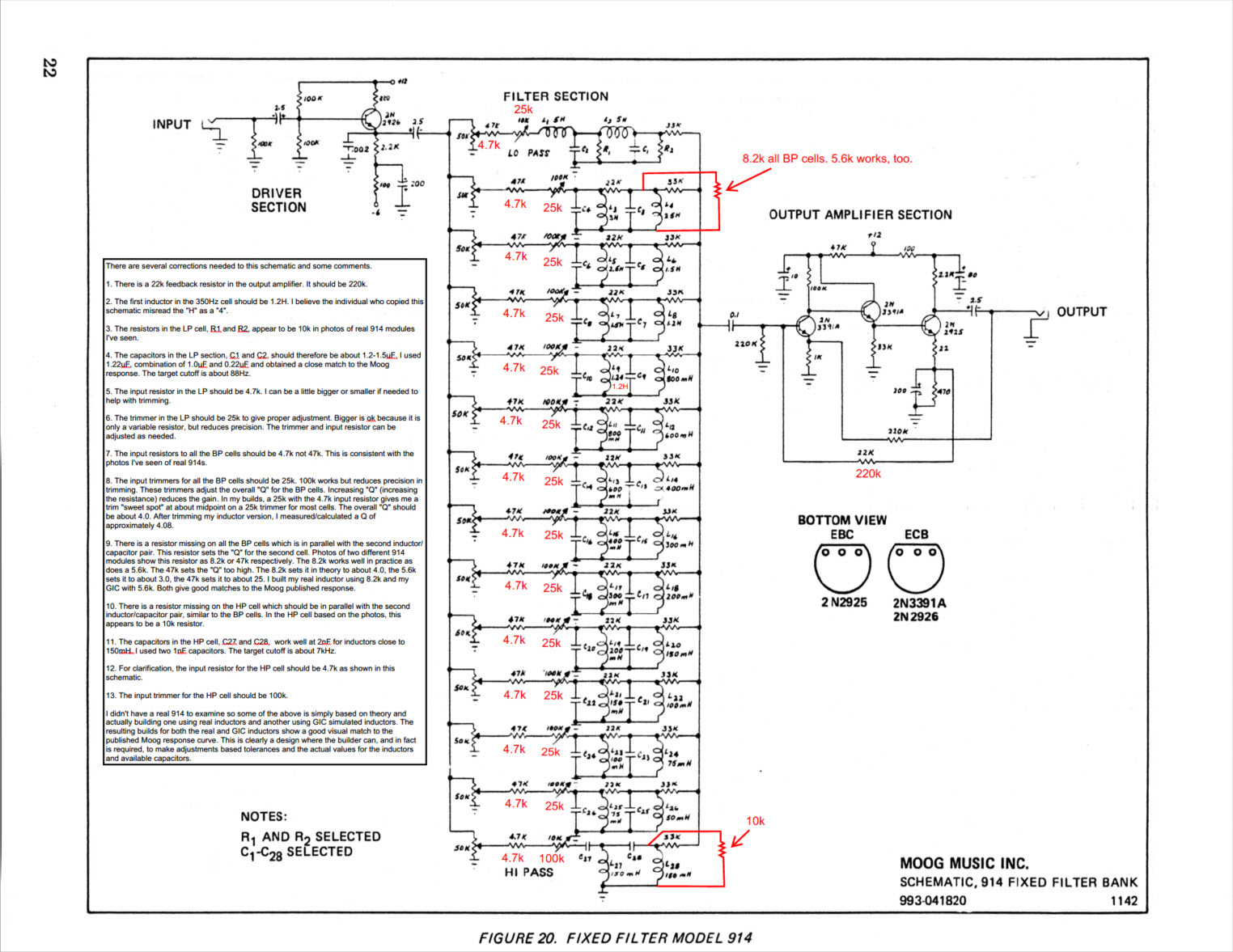
Moog 914 FFB schematic from the Norlin service manual. The notes in the box and in red are mine.
Work sheets for calculating the capacitance:
These pages show the formulas I used and the calculations for the capacitance needed for each stage in each band pass cell. I first calculate a spread for the frequency, first stage 6% lower than the specified cell’s center frequency and the second stage 6% higher. I then calculated the capacitance using the actual measured inductance of the coils I used and then assuming the ideal Moog specified inductance.

This is simply the calculation of the spread for the center frequencies for each stage of each cell. These are used when calculating the needed capacitance in each stage of each cell.

This page shows the calculation of the capacitances using the inductances I measured in my build. It is interesting to compare the results with those assuming the ideal Moog values.The first stage’s center frequency is 6% low and the second stage’s is 6% high.

This page shows the calculation of the capacitances assuming the inductors are the ideal Moog specified values. The first stage’s center frequency is 6% low and the second stage’s is 6% high.
Calculating the resistor for the second stage in the BP cells to set the “Q”.
In all the photos I’ve seen, it is clear there is a resistor in parallel with the second inductor in each BP cell and in the HP cell (the photos of the HP cell consistently show a 10k resistor in the HP cell). This resistor sets the “Q” for the second stage and this “Q” should be around 4. The trimmer sets the “Q” for the first stage as well as affecting the overall “Q” and gain. This sheet shows the formula I used and the calculations for a target “Q” of 4, or the “Q” using a resistor of 8.2k. I also used the ideal inductance and capacitance for the calculation. In the end, I think the 47k I saw in some photos is simply too high. It gives a “Q” of about 25 for the second stage and the peaks are too sharp and don’t allow the spread in the pass band that is seen in the original Moog frequency response, see below. Something in the range of 5.6k to 8.2k yields good results.
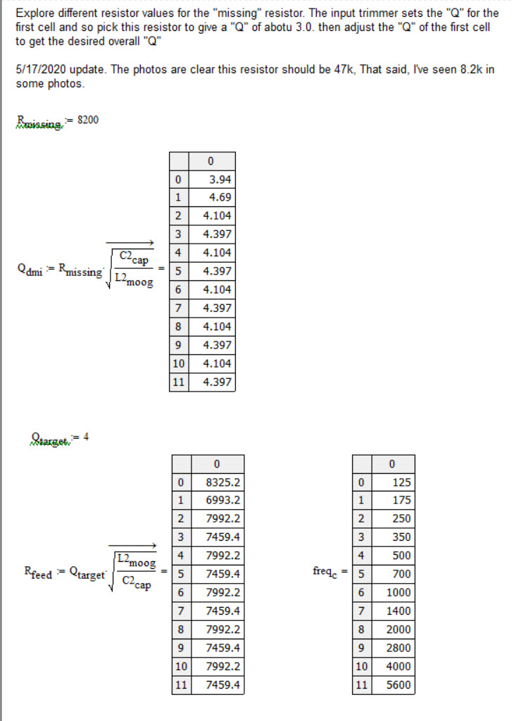
This page shows how to calculate the “Q” given the resistor value or the resistor value given a “Q”. I noticed that in one 914 for which I had photos, Moog had used a 47k resistor in parallel with the second inductor in each BP cell. In another, it was 8.2k. I tried as low as 5.6k with good results. The larger the resistor, the higher the “Q”, the sharper the peak, and the higher the effective gain of the cell. I personally think a lower “Q” more closely matches the intent and published response curve.
Work sheets to choose capacitors:
Here are Excel spreadsheets and PDF versions of a table to help you pick capacitors. I took standard values, 5% tolerance, between 1nF and 1000nF (1uF) and combined them in pairs for every combination. One set omits 7.8nF because I couldn’t find the right lead spacing.
For example, if you need a 257.3nF capacitor (purely a random choice) having calculated the center frequency for one stage of a cell based on your real inductance, look at the table and you will see two or three choices that are close. On the table, there’s a 253nF combination (33nF and 220nF) or a 262nF (180nF and 82nF). Sometimes, there are two combinations which produce identical values, just choose the one for which you have capacitors. Remember, too that the nearest value is sometimes just a single capacitor.
These first two files omit the standard 7.8nF capacitor because I couldn’t find one with the right pin spacing.
Cap combinations without 7.8nF Excel file
Cap combinations without 7.8nF PDF file
These two files include the 7.8nF value in case you found a 7.8nF with the proper pin spacing.
Cap combinations Excel file
Cap combinations PDF file
PANELS:
Grayscale was offering a group panel buy of his design which is quite stunning. See here: Grayscale Group Panel Buy. Here is a link to the Front Panel Express panel layout: Moog_914_FFB_Panel_03
UPDATES:
- Added more information to the documents archive. Please download the newest version.
- Added some clarification on the polarized capacitors in the Power section.
- Added some links and a little more about connecting the “DRIVE” signal between PCBs.
- See below under “Inductors” for details, but Carsten is not winding the inductors at present but the ones Moog is using in their re-issued systems are available on special order from CineMag. I re-laid out the PCBs to reflect this. Let me know which inductors you are using so I can supply the correct PCBs.
- THE GIC PCBS HAVE NOT CHANGED AND REMAIN AT THEIR CURRENT REVISION LEVEL. ONLY THE INDUCTOR PCBS HAVE CHANGED AND AT SOME POINT NEW INDUCTORS PCBS WILL BE OFFERED. PLEASE INQUIRE.
- NEW DOCUMENTS UPLOADED. SEE ABOVE.
- I AM BUILDING A NEW PROTOTYPE FOR THE CINEMAG INDUCTORS. THIS IS COMPLETED AND IT WORKS GREAT!
Corrections:
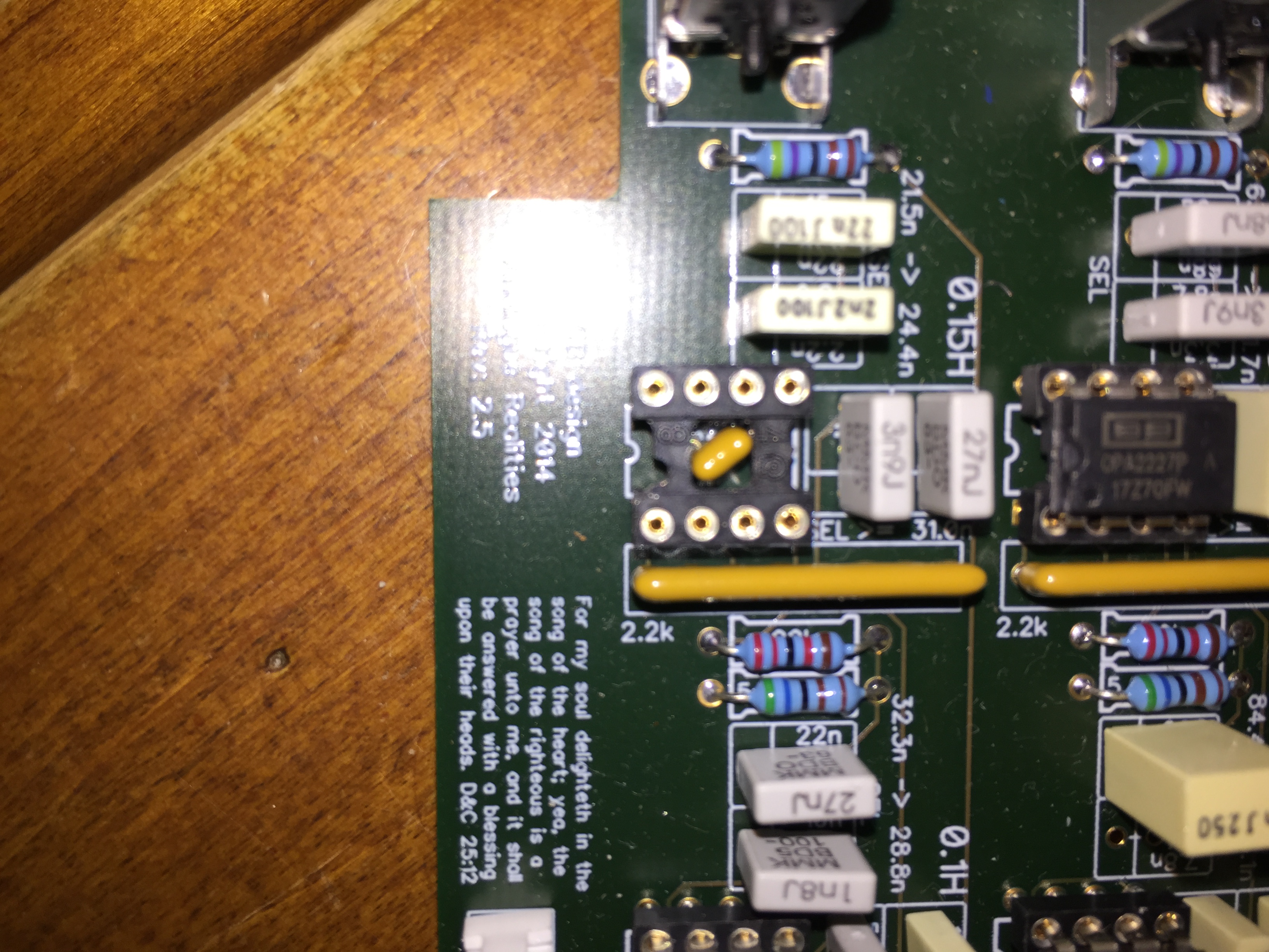
- In both the GIC and inductor versions, the 22k feedback resistor in the output amplifier section should be 220k as is the other feedback resistor. That is, R222 and R214 should be 220k. Thank you Dave Brown.
- In both the GIC and inductor versions, remove the HP filter I put on the input to the EVEN and ODD output amplifiers. Do not install R311 or R411 and put a jumper in place of C301 and C401.
- In the GIC version only, the two summing resistors for the Low Pass cell need to be larger, 390k is perfect. There is one for the ODD summing point and another for the ALL summing point. These are noted on the PCB silk screen as LP 33k/130k. They are resistors R403 and R207. If you use the specified 130k, the gain on the Low Pass cell is much too high. Please use a 390k. On the inductor version, use the 33k like in all the other cells.
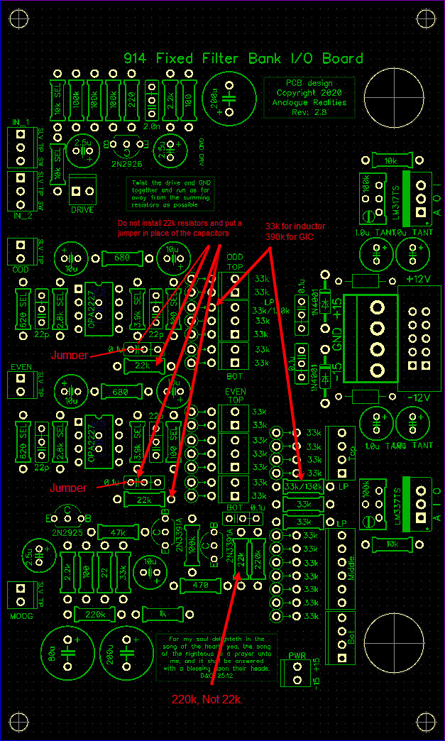
I/O PCB showing corrections. NOTE: This image is a Rev 2.8 PCB. The only change from 2.7 was the physical size of the PCB. The changes indicated work with the 2.7 PCB as well.
- In both the GIC and inductor versions, for the resistors marked as 5.6k which are in parallel with the second inductor in each BP cell, I’ve looked more closely at the photographs and I identified that in one version of the 914, Moog’s™ used 47k resistors in parallel with inductor in the second stage of each band pass filter cell. On another version, these resistors were 8.2k. The difference is the 47k gives the second stage a “Q” of 27, the 8.2k about 4. In my GIC version, I used a 5.6k which is a “Q” of about 3. It makes a different in trimming the cells as well as the response of each cell. With the 47k resistors, the peaks are sharper, a higher “Q”. With the 8.2k or 5.6k, the peaks are more rounded, a lower “Q”. Looking at Moog’s™ published 914 response, I think the best match is with the lower values. The correction is that you can use the marked 5.6k or up to an 8.2k.
- In the inductor version only, the capacitors in the LP cell need to be about double what is in the schematic and written in the silk screen. I used 1.22uF; a 1.0uF and 0.22uF capacitor in parallel. A 1.5uF also works but starts to push the cutoff frequency to low.
- In both the GIC and inductor versions, the capacitors in the HP cell should be a little bigger. I used 2nF. 2.2nF could also work. For 2nF, use two 1nF capacitors in parallel. For 2.2nF, just use one 2.2nF capacitor.
- In both the GIC and inductor versions, the trimmer for the HP is “backwards”. Turning it CW decreases the “Q”. There are three fixes:
- The first is the easiest I think. Leave it and just remember it is opposite the other trimmers, :)
- Next, you can replace it with a trimmer with “crossed” pins. The trimmers called out are a 3362 type “X” trimmer. Pin #1 is on the left when looking at it, and pin #3 is on the right. You can substitute a type “W” which reverses these two pins so #3 is on the left and #1 is on the right. See the photo below. It shows the “W” type on the left of the photo and an “X” version on the right. The only quirk with the “W” trimmer is the indicating “arrow” is rotated 180 degrees so at mid-span, the arrow points down instead of up. This is the correction I chose because I had a bunch of “W” type trimmers.
- Last, you can cut the trace connecting the wiper (pin #2) to pin #1, the left side looking at the trimmer, and then install a jumper from pin #2 to pin #3.

A 3362 type “W” on the left. A 3362 type “X” on the right. Note the pin numbers and locations at the bottom corners of each trimmer.
Frequency Response
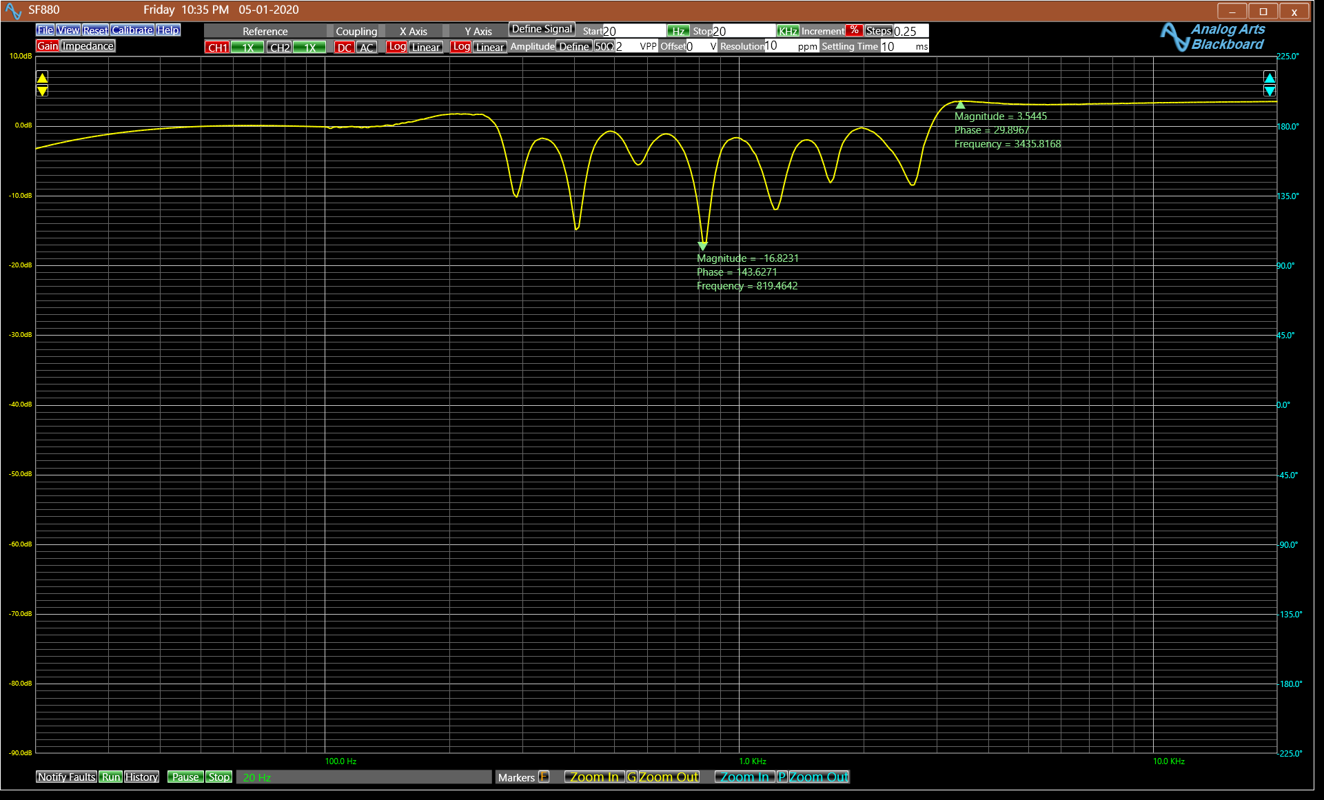
Here are plots of the frequency response of the real inductor version and GIC version. I’ve included a better resolution copy of the Moog™ published 914 response, too.
The analysis was done with an Analog Arts FS990 “Sub-Hertz” Sweep Frequency Response Analyzer (SFRA). What an amazing tool! Besides the SFRA function, it has an oscilloscope, spectrum analyzer, data recorder, arbitrary waveform generator, logic analyzer, pattern generator, and frequency/phase meter. They have exceptional technical support and the quality of the instrument is the highest. Not paid, just a very happy customer. Here is a link: Analog Arts FS990.

Moog 914 frequency response published by Moog.
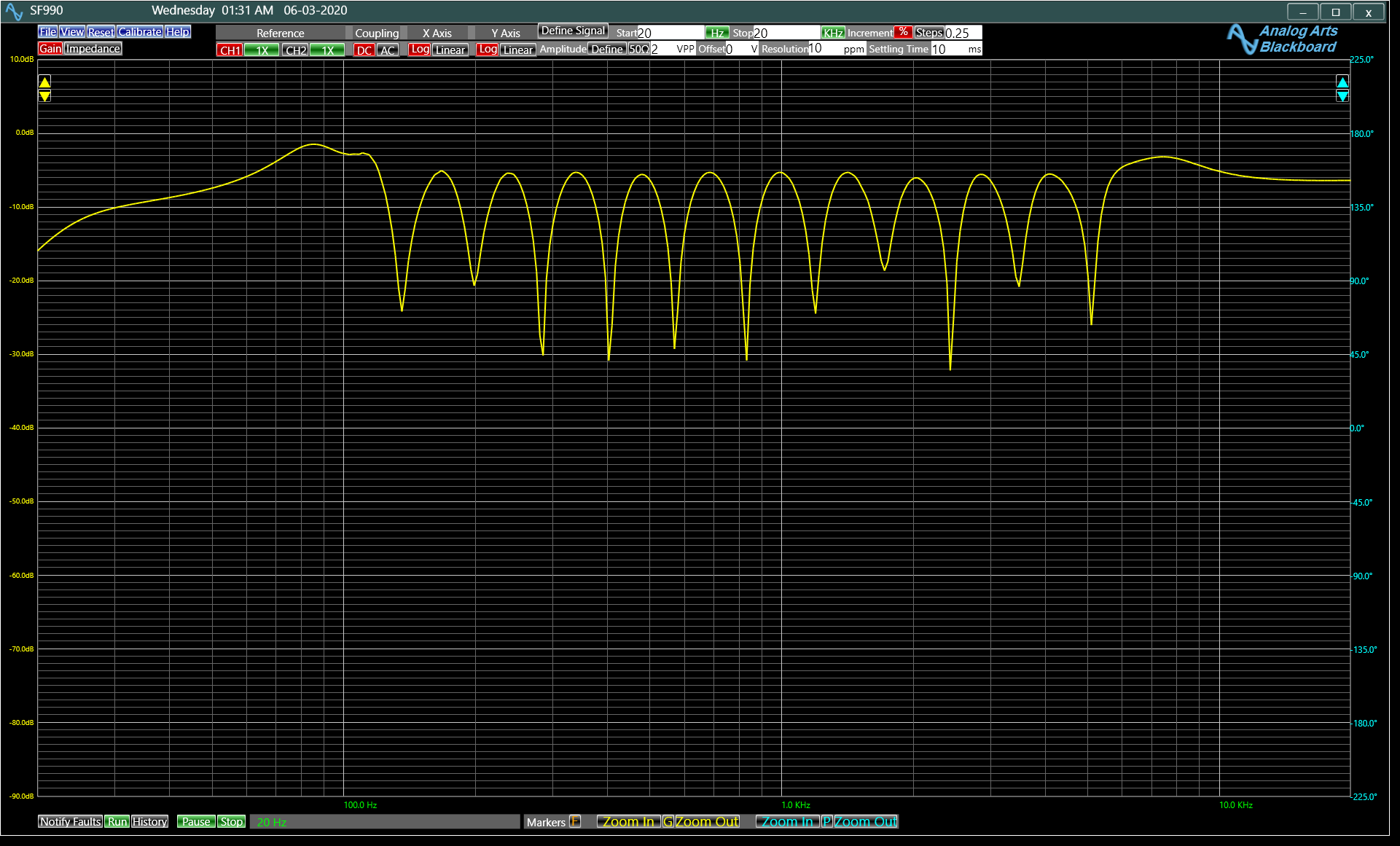
Frequency response of the 914 based on GIC inductor simulators.

Frequency response of the 914 based on real inductors.
For fun, I did a frequency response analysis on the Moog™ 907 from my Model 15 re-issue. I was intrigued by the result.

Moog 907 frequency response.
Measured frequency response of my Moog 907.
INTRODUCTION:
First, I have to give credit where it’s due for the inspiration.
- Dr. Moog and his engineers for the original design.
- Yves Usson for his work, design, and idea to break out even and odd cells.
- Jurgen Haible (R.I.P.) for his approach using simulated inductors (GIC)¹.
My design clearly derives from the original Moog™ design and is as faithful to that design as possible. I spent more time pouring over those simple filter circuits more than any other project I’ve undertaken. Hours of simulation in MultiSim trying to characterize the circuit. Staring at photos and trying to trace signals and identify components. Finally realizing a resistor was missing which made all the difference because the resistor directly helps determine the “Q” of the cells. Then the reward of simulations that produced the proper frequency response and prototypes that finally worked the way they should with very little noise or hum. Last, dealing with some form and fitment issues so that the module could reasonably be built. What a trip.
So, thank you Dr. Moog, Yves, Jurgen, and any teacher or author who taught me, and especially my dad who taught me to love electronics as soon as I could hold the solder for him while building Heathkits.
The project is not cheap. Plan on $300.00 or a little more for inductors, and depending on what you choose, as much as $130.00 for op amps (see below). The GIC version is pretty straight forward to build and probably more robust if you gig your synthesizer. The inductor version clearly will be more true to the original, but soldering the extremely fine varnish coated wires and getting a solid solder joint takes patience and care. The cores are a bit brittle and fragile and care must be used when mounting them. In the end though, you will have an extremely useful and unique module for sound shaping.
Don’t hesitate to ask questions or give me feedback. I don’t do this to make money. I just want to help you make the music that I don’t have the talent to make myself.
FUNCTION:
This module is not an equalizer but it does boost and attenuate in frequency bands, so it is an equalizer. Honestly I don’t know what to call it. Reading the information I could find, mostly from the MoogArchives.com website (the following is in part paraphrased from the Moog™ docs reproduced there), this filter is a non-voltage controlled “modifier” with 14 band pass filters with a control which adjusts the level of each band. Each band has a 12dB slope. This creates peaks and troughs similar to a formant filter. There is also a low pass band and a high pass band.Each band has a “Q” of about 3.7 (thank you Yves for that tidbit). I think the intent was specifically for it to be not voltage controlled so that the timbre of an input signal would change as it moved through the frequency regions. One use might be to help replicate the fixed resonances of a particular real instrument, or for creating other unique effects by emphasizing certain bands mixed with an unfiltered signal.
USE:
A modifier module, typically in near the end of the signal path before final mixing, but it can go anywhere you have an audio signal to process. It is ultimately AC coupled so it is not of much use for CV processing. You can use the filter as an “all pass” filter and send the even signal to one stereo channel and the odd signal to the other for an interesting pseudo stereo effect.
Inputs/Outputs:
There are two inputs:
- Signal. The summing resistor on this input can be chosen to handle higher level signals than originally intended by Moog™ or just high signal levels in general.
- Signal. Same as for #1. There are two summing resistors on the PCB so you can choose these to suit your needs. One big, one small so you can handle and mix both high and lower level input signals. I picked a relatively large summing resistor because my audio signals are typically higher than in the original.
There are three outputs:
- Main Signal. This is the sum of all the filter cells amplified back to line levels.
- Even Signal. This is the “even” filter cells starting with the 125Hz cell and summing with every other cell up to and including the HP cell.
- Odd Signal. This is the sum of the “odd” filter cells starting with the LP cell, summing every other cell ending with the 5600 Hz cell.
Knobs:
This module has 14 knobs (pots) which control the attenuation of each cell.
Switches:
There are no switches
GENERAL CONNECTIONS:
Connect an audio signal you want to process to one of the inputs, or both if you want to mix them first.
COMPONENT SELECTION:
See the Component Notes page for some general information. See below for specific information relating to this module.
Resistors:
Use good resistors like metal film, as that will help keep the noise down
Capacitors:
Use high quality capacitors, like a polyester film type especially for the GIC version in the GIC cells. Harry Bissell has a great capacitor reference reproduced here if you want to learn a bit about the different types and uses for capacitors.
 The decoupling capacitors can be mounted on the underside (GIC version only) or in the DIP socket, if you use a socket. If you want to put the in the socket like in the photo, make sure you get a physically small, MLCC type. If you mount them on the solder side, do them first. Otherwise, good luck soldering them with an IC in the way…
Each capacitor which helps set the center frequency for the filter cell along with the inductor, real or GIC, and the capacitors which help set the value of the simulated inductors (GICs) is made from two capacitors in parallel if needed and there is room for two capacitors with two different lead spacings ( 0.1 or 0.2 inch (2.5mm or 5mm)). Moog™, Yves Usson, and Jurgen Haible do it this way, so why buck the system? I printed two values on most capacitors in different directions. I’ll explain why and how to pick the right values.
It appears that Moog™ designed the center frequency (CF) of the first cell to be a bit lower than the target CF and the CF of the second cell to be a bit higher. I have no proof of this other than looking at the schematics for the 907 and Jurgen’s design. Yves uses the same CF for the first and second cell. To do this, the capacitor for the first cell should be a bit bigger than ideal, and the capacitor for the second cell a bit smaller. But, if you think it is better to have the same CF for both cells, you can do that, too. I calculated values for either way.
If you look at the build photos, you’ll notice that on the GIC PCBs, there are a couple of capacitors whose value is not visible. For reasons I don’t understand, the value on this 180nF capacitors was printed on the side. It was only on these capacitors. You will also note the actual filter capacitors are the same on the inductor version and the GIC version. The GIC version has extra capacitors to help set the inductance value.
Remember that capacitors in parallel simply add their capacitance together.
On the PCB, you will see markings adjacent to the capacitor pairs that look like this from the first cell in the 175 Hz filter
330.8n -> 374.4n
This means the ideal capacitor is 330.8n and can move towards a value of 374.4n to achieve an CF that is 6% lower than ideal. The second cell is marked
551.4n -> 490.8n
which means the ideal is 551.4n but you can reduce that to 490.8n to get a CF 6% higher than ideal. Your combination of capacitors should add up to a value somewhere between these two numbers.
The GIC is similar, but since the GIC is the inductor, you want the capacitor to create an inductor of the ideal value, or err on the side of pushing the CF down for the first cell (bigger inductor), or up for the second cell (smaller inductor). These capacitor pairs are marked like this from the first cell in the 175 Hz cell
SEL >= 516.5n
which means create a combination of capacitors to be greater than or equal to 516.5n
The second cell is marked
SEL <= 309.9n
which means to create a combination of capacitors to be less than or equal to 309.9n
All right, you say thanks David for doing the math, but what two capacitors do I choose? “Ahhhh,” I say. “Look at the capacitors values on the silkscreen and you will see your answer.” On each of the two capacitor pairs, there are two sets of values. You should be able to tell which ones go with the ideal value and the 6% offset value by adding them together. The values on the left side of each capacitor are the ideal, and the values on the right side of each capacitor are the 6% offset. For the GICs, there is only a suggested combination for the ideal which is either “greater than or equal to” for the first cell or “less than or equal to” for the second cell.
Sometimes, there is only one value printed on a capacitor. That’s because using only one capacitor was the closest solution.
The printed values are standard values for polyster capacitors you will find at the lin k I gave you above. There are two lead spacings you can use on the PCB, 0.1 or 0.2 in (2.5mm or 5mm). There is a little capacitor symbol between two of the pads. If you use the smaller spaced pads, make sure your capacitor spans the two holes that are on either side of the symbol. It looks like this:
o-o||o
On this example above, you would put the capacitor in the two pads on the right side. The link I gave takes you to the 5 mm spacing, so there is no problem. You are welcome to do your own calculations and pick your own values. I arrived at these by creating a table of the combinations of most of the standard values available and simply hand picked the ones which best met the criteria. I’m sure there’s a smarter way to do it…
Email me if this is too confusing.
Inductors:
If you build the inductor version, you need inductors. You can wind them yourself (it’s SDIY, right?) or you can get them from Carsten . He has this all figured out and he will gladly send you a set of hand wound inductors to work in this module. If you do the GIC version, the inductors are simulated with op amps.
Should you happen to break a core, Carsten will sell you new ones or I found these ones from Mouser work at least for the small inductor size Carsten sells Small Inductor Core and these for the big ones, Big Inductor Core.
Note, it appears Carsten is not making these at the moment. However, you can get the same ones Moog is using in their re-issued systems from Cinemag. They are not listed on the site, but use the contact page and they can help you out. The part numbers for the inductors are:
The following are a small, apx. 22mm diamter form factor:
- CML-4811-1 Inductor 50mH
- CML-4811-2 Inductor 75mH
- CML-4811-3 Inductor 100mH
- CML-4811-4 Inductor 150mH
- CML-4811-5 Inductor 200mH
- CML-4811-6 Inductor 300mH
- CML-4811-7 Inductor 400mH
- CML-4811-8 Inductor 600mH
- CML-4811-9 Inductor 800mH
These are a larger, apx 26mm diameter form factor:
- CML-4811-10 Inductor 1.2H
- CML-4811-11 Inductor 1.5H
- CML-4811-12 Inductor 2.5H
- CML-4811-13 Inductor 3.0H
- CML-4811-14 Inductor 5.0H
They are excellent quality. They are a bit expensive and you may have to pay a setup cost, but they are really worth it. You will also see there is no 1.24H inductor. Apparently Moog did not use the 1.24H in their re-issued systems in contrast to what is in the Norlin Schematics. Personally, I suspect the Norlin schematic was simply wrong as they are in so many places. I detailed other errors in the 914 schematic herein.
I redesigned the PCBs to fit the CineMag inductors. Let me know which inductors you are going to use and I can ship the proper PCBs.
Be sure to measure your inductors and adjust the capacitors as/if needed. The values on the PCB assume the specified inductance for the calculations.
ICs:
First, there are two ICs on the I/O PCB. These can be any decent generic op amp. They are labeled and the BOM calls for a OPA2227 which is a very, very low noise, expensive op amp. These are really overkill.
The output amplifiers for the Even and Odd cells are not part of the original 914, so use what makes sense to you. For example, an NE5532 would be fine.
Second, the GIC cells. GICs are prone to noise. Picking a cheap op amp here is a bad idea. You will pay the price with noise. Jurgen Haible specified a 4558 op amp. I specify an OPA2227 (or here at twice the price) which is a very, very low noise op amp and I’m really happy with how quiet the GICs are with these. They are expensive however, and (including the I/O PCB) there are 29 op amps in the GIC version. At $4.50 each, that means $130.50 just for the op amps. The 4558 is about 1/10 that cost. It’s your module, you be the judge. Just remember, you have several noise sources in the signal path ahead of the output amps, and the output has a gain of about 270. The more you can reduce the noise in the filter cells, the better. I can’t do much for how the Moog™ output amps works because I don’t want to change it. The Even and Odd output amps use a two op amp cascaded design in an effort to reduce noise.
Transistors:
The original used 2N2926, 2N3391A, 2N2925 transistors. The 2N2925, 2N3391A transistors are still made and can be had at Mouser. The 2N2926 is harder to find, but not anywhere near impossible. Honestly, I can’t tell you why Moog™ used three different types of transistors in the circuit. The 2N2926 is in the input stage. I see no reason why you can use any reasonable low noise, small signal transistor here. The output stage should have high quality, very low noise transistors due to the high gain in the stage. The 2N2926 is available at Cricklewood Electronics and maybe some other places, too.
Pots:
The PCBs are laid out for a Panasonic PCB pot available at DigiKey and other sources I’m sure. Panasonic # EVU-E2JFK4D54, DigiKey # P3U0503-ND. You will probably have to trim the shaft, I did anyway. I used a Dremel and a cutoff wheel.
You will also need a couple of small’ish panel mount pots for the low pass and high pass attenuators. The hole in the panel design is made for an Alpha pot. If you choose a different one, be sure to check the mounting hole diameter. The top PCB is notched to accommodate these two pots.
Trimmers:
There are 14 trimmers. I specify a Bourns 3362X series. This is a single turn trimmer. The foot print will fit many different trimmers, just be sure the trimmer is set up so that when you turn it clockwise, it connects to the right hand pin as seen when looking at the PCB from the rear (see the PCB layout). Some Bourns trimmers will connect to the pin on the left when you look at the trimmer adjustment.
Jacks:
For the panel I laid out, a good 3.5mm or 1/8 inch jack will work. I use the Switchcraft 42A Tini-Jax true 1/8 inch jack. These are switched jacks and they work with 1/8 inch plugs and 3.5 mm plugs. There are a lot of good 3.5mm jacks which will work.
Switches:
There are no switches.
Connectors:
I provided locations for standard 0.1 inch pitch MTA connectors or you can just solder the wires. I highly recommend you do not solder both ends. On the GIC version, the connectors all mount on the component side and you can use vertical connectors. On the inductor version, due to how I laid out the PCB, you need to mount some of the connectors which would otherwise block access to the trimmers on the solder side. Also, I recommend you use 90 degree connectors on the bottom filter cell PCB and mount them on the solder side as indicated. It’s a tight fit, and you can mount them on the component side, too like I did in this prototype.
What’s important is that you connect the Even to Even, Odd to Odd, and All to All between the filter cell PCBs and the I/O PCB. The order of the cells makes absolutely no difference, so don’t worry about the order of the pins, with one big exception on the GIC version…
TAKE NOTE ON GIC VERSION: The output of the low pass filter cell on the GIC is substantially higher than for the other cells. It’s summing resistor has to be much higher, about 390K* as opposed to 33K. You must make sure that the pin connected to the low pass signal connects to a 390k (adjust to your taste) summing resistor on the I/O PCB. You have to do this for the “ODD Cells” and for the “ALL Cells” connector. It’s marked on the I/O PCB, but I forgot to add it to the silkscreen on the middle cell PCB. On the ALL and ODD cell connectors, it’s the pin on the far right, opposite end to the square pad. If you get this wrong, the low pass cell will be extra loud and what ever cell you connected to the 390k will be very, very quiet.
This is not relevant for the inductor PCB. The summing resistors are all 33k so the order doesn’t matter. Just be sure to connect the “ALL” connectors on the inductor PCBs to the “ALL” connectors on the I/O PCB and the “EVEN” connectors and “ODD” connectors to the respective “EVEN” and “ODD” connectors on the I/O PCB.
Here is a Mouser link to the type of 90 degree connector I used. This is the three pin version. Other links are on the Component Notes page.
*This is a revised value. See the UPDATE section at the top of the page.
BUILD NOTES:
Here is a link to the page with build photos for the inductor version. A link to the GIC version will follow. The pages are also a sub-page to this one in the menu to the left.
Soldering:
I assume you know the basics of soldering. I like to insert the low lying parts first, like resistors, diodes, etc. After these, I install the IC sockets. Next capacitors, transistors, connectors. Use a good solder, either an organic flux, which you should wash regularly, or a no-wash flux.
Take a break every so often, wash off the flux if you are using a flux which required cleaning. Double and triple check orientations, pins, and solder joints.
Power Supply Regulation/Filtering:
The module needs +12 and -6 volts. I use adjustable LM317 and LM337 regulators to convert either +/- 15 volt or +/- 12 volt supplies to the proper voltage levels. Per the data sheet, the regulators should have a 0.1uF ceramic on the input and a 1.0uF Tantalum on the output. I added a 1.0uF Tantalum on the input to help filter a noisy main supply. NOTE: These four filtering capacitors, C503, C504, C506, and C507 can also be 10uf electrolytic capacitors per the data sheets.
You can probably always omit C503 and C506 with no bad effect (the polarized capacitors on the input side).
You can use either +/-15 or +/-12 as a main supply. If you use 15 volts, you will need both regulators. If you use 12 volts, you just need the negative regulator (LM337). Obviously, if your main supply is +12 and -6 volts, you don’t need either regulator. If you omit a regulator do the following:
- Put a jumper between the “I” and “O” pads.
- Omit the trimmer and the associated fixed resistor. R501 and F502 for positive and R503 and R504 for negative.
- Omit one of the polarized capacitors, otherwise you’ll have two capacitors in parallel. This won’t hurt, but it’s not needed. Omit either C503 or C504 for the positive side or C506 or C507 for the negative side.
If you do the power supply first (good idea) remember, you have to have a sufficient load on the regulator to make it regulate, like 10mA. So, if you do the power supply section first, you will also have to connect a temporary resistor between the output and ground sufficient to draw about 10mA (R = E/I or 12/0.01 = 1.2k, or for the negative side 6/0.01 = 600 ohms). Again, just be careful. Don’t hook up the filter cell PCBs on the GIC version or install the output amplifier op amps (especially if you use the expensive ones) until you’ve checked the supply voltages.
TAKE NOTE ON THE INDUCTOR VERSION: There is no power needed on the filter cell PCBs so you don’t need to install a 2 pin power connector on the I/O PCB. However, you should connect the ground wire of the DRIVE connector between PCBs to make sure they all have a ground reference.
TAKE NOTE ON THE GIC VERSION: There are several two pin power connectors which need to be daisy chained between the PCBs. Make sure each PCB has power.
COMPONENT PLACEMENT:
Mounting:
The PCB pots mount all but the I/O PCB to the front panel. The I/O PCB has different holes so you can choose to mount it with spacers to the panel or to the bottom filter cell PCB. You can look at the photos of my build to see what I did. Keep in mind different clearances with all the connectors, etc. as you mount and run wires.
You ask, why the two big holes at the back of the I/O PCB and why the big rubber feet? My rack has a mesh metal bottom and the I/O PCB was very close to the mesh. I didn’t want a short, so I added to two big holes to fit some BUD press in rubber feet just to make sure I didn’t short. You don’t have to use the feet, but a photo of the Mouser bag is included in case you do.
IMPORTANT: The signal level at the summing node for the filter cells is very low and the signal level in the “Drive” signal wires is high. The inductors are also susceptible to stray electromagnetic fields. Run the “Drive” signal wires as far from the summing nodes and inductors as feasible. I drilled holes at the front of the PCBs to help with this. You can also twist the wires which should help. You can also use a small flexible shielded cable (what I did) on the inductor model which will help, but is a bit of a pain.
UPDATE
I have updated the inductor PCBs to accommodate the CineMag inductors. I found that using regular hook-up wire was fine and I hear no noticeable noise or hum. I would suggest that Coax is not necessary.
Calibration:
Wow… where to start. In theory, the calibration is very simple. Turn the trimmers clockwise to increase the “Q”. A good starting point is between about 10:00 and 12:00 Remember the behavior of the HP trimmer will depend on if you corrected it and how you corrected it, see above in the corrections and below. The following image shows you where I trimmed mine when I was done. Most of them are around 11:00. The exceptions are the high pass is just past 12:00 (mine is upside down, a “W” type), the 5.6kHz is at about 2:00, and the LP is just past 12:00 about the same as the HP.
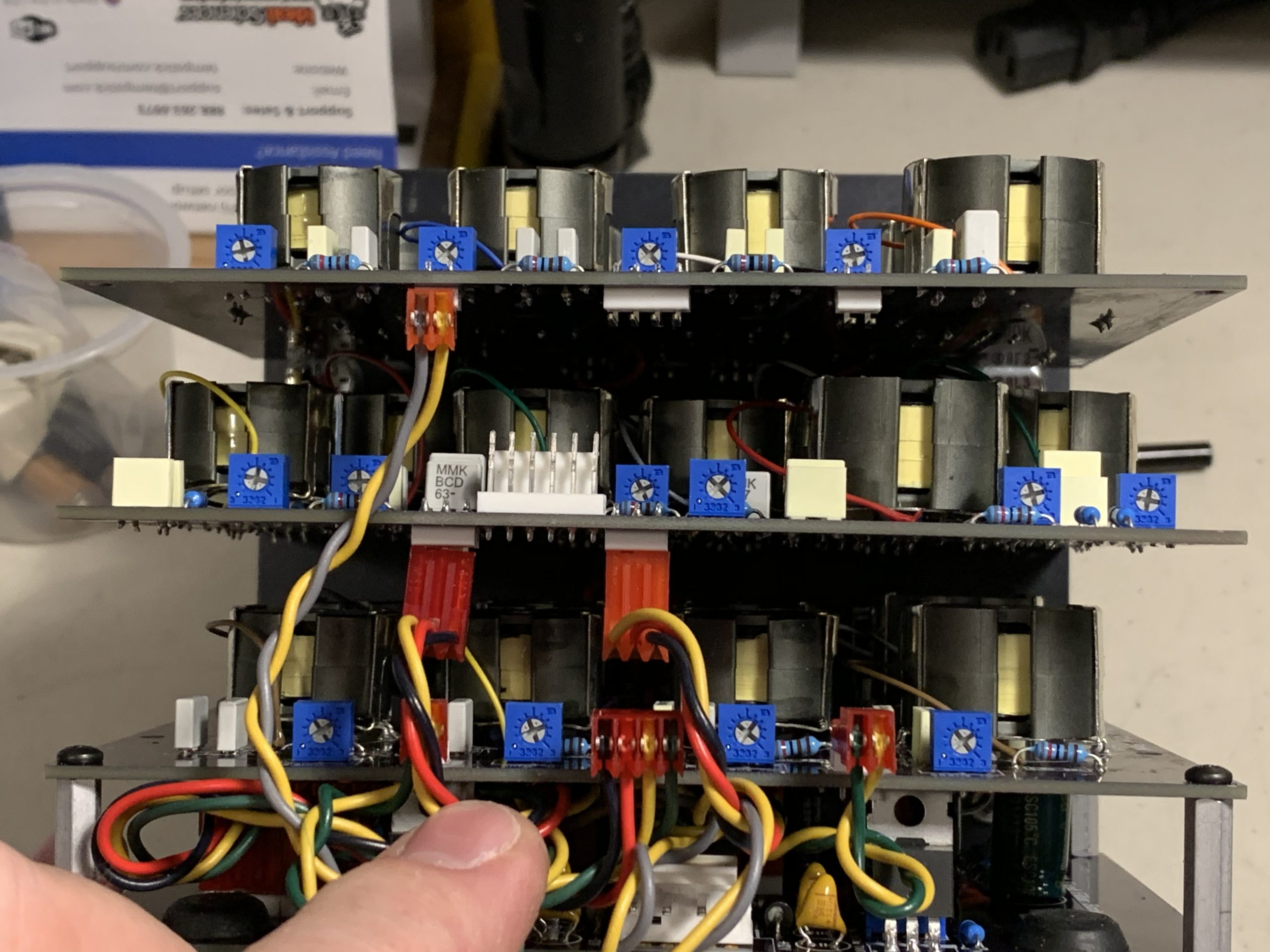
This shows the position of all the trimmers when I was done. Note that on the middle PCB, left side, the HP trimmer I used is a “W” type. The indicating arrow is rotated 180 degrees as compared to a more standard “X” type. This means that mid-span the indicator points down. In other words, 12:00 is pointing straight down. I did this to make the CW rotation increase the “Q”. See the notes for more. Some cables were disconnected to allow a better view of the trimmers.
In practice, you need some way to measure the frequency response of each cell. As noted above, I used an Analog Arts FS990 Sweep Frequency Response Analyzer (FSRA) to tune my latest inductor and GIC versions. Analog Arts FS990. I followed this process. Based on a visual estimation from the Moog™ graph, I chose a target magnitude for each BP cell and the LP/HP cells. I turned the LP and HP cells off and ran an analysis. I adjusted each of the trimmers in an effort to get the peak magnitudes to my target, -6 to -7 dB. I then added in the LP and HP cells and trimmed them to get a maximum magnitude of about -1 or -2 dB. Moog™ claimed an overall gain of 0 dB, but it is clear in their plot, the magnitude of each cell is below 0 dB with the LP/HP between 0 dB and -5 dB. The BP cells bounce around -6 dB to -8 or -9 dB. In the end, I’m happy with my tuning and performance. When I was done, I also calculated the “Q” for the 1kHz cell. I based the calculation in RaneNote, #170, author Dennis Bohn from the RANE Corporation. The simple spread sheet the author referenced is also provided below. As far as I know, the paper and spreadsheet can be distributed, if this is incorrect, please tell me and I will remove the links. I’ve run the spreadsheet and there are no viruses, but be safe and check all archives for malware and viruses before you open or execute them. The spread sheet has my numbers in it.
Remember, CW increases the “Q”, CCW decreases the “Q” and note that increasing the “Q also attenuates the signal going through the cell, so clockwise also attenuates the output for that cell. I also found the trimmer for the HP cell is backwards. This can be corrected by using a “W” type trimmer instead of an “X” type.
Quick story. A good friend bought a Ferrari 308. He also owns and hot rods Porsche 914s (hmmm, no relation to this module :) ) he told me about the difference in tune ups between the two. The German Porsche had very precise and clear metrics and instructions for tuning the engine. The Italian Ferrari manual, on the other hand, would say “turn this screw until is sounds right” or “adjust this control until it feels smooth”.
In the spirit of Ferrari, adjust the “Q” to your liking. The original 914 had a “Q” of about 4.0 in each cell (thanks to Yves’ research and analysis), so if you want to have the Porsche version, you can do it, but you will need a frequency response analyzer. You can buy a dedicated device like I did, or some oscilloscopes have the function built in, e.g. some of the Keysight scopes.
PANEL NOTES:
There is nothing too special. I suggest using connectors on the flying wires from the jacks and pots to the PCB.
The mounting holes and spacing are setup for Alpha 16 mm or 12 mm pots. The jack holes are 0.25 inch in diameter.
————————————————————————————————————————————————————-
1. There are a lot of references for Generalized Impedance Converters and some configurations other than what I used here. If you want some, let me know and I can send you some references. Otherwise an internet search will pull up some interesting information.